In 2022, the Government of India announced,
The India Semiconductor Mission (ISM) to establish itself as a global player in the Semiconductor market to reduce import dependence by about 90%. India aspires to create a local pool of knowledge, to expand its economy. The intentions are good, the GOI has also announced a handsome budget for the initiative. However, the policy is not grounded in the realities of the global Semiconductor Industry and the future direction of technology development.
ISM comprises four schemes
1 Setting up of Semiconductor Fabs in India. GOI to extend fiscal support of up to 50% of project cost. With an initial budget of US$ 9 Billion.
- Setting up Display Fabs in India. GOI shall extend fiscal support of up to 50% of the project cost.
- Setting up of Compound Semiconductors / Silicon Photonics / Sensors (including MEMS) Fabs / Discrete Semiconductors Fab and Semiconductor ATMP / OSAT facilities in India. Fiscal support of 50% of capital expenditure.
The nodal agency of these three scheme’s is Ministry of Electronics and Information Technology (MeitY). - The Design Linked Incentive (DLI) Scheme aims to offer financial incentives as well as design infrastructure support across various stages of development and deployment of semiconductor design(s) for Integrated Circuits (ICs), Chipsets, System on Chips (SoCs), Systems & IP Cores and semiconductor linked design(s). The nodal agency is C-DAC (Centre for Development of Advanced Computing) a Government body.
Here are some issues:
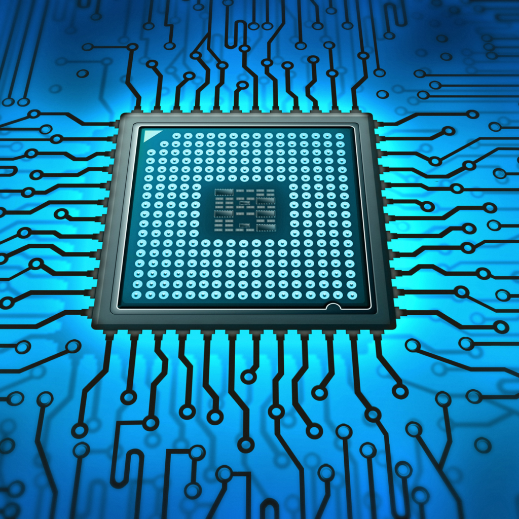
Items 1 to 3 have tremendous installed capacity the world over with more plants under construction as a hedge against China’s conflict with Taiwan, the US-China Chip war and a concentration of manufacturing in South East Asia. These plants are extremely capital intensive and obsolescence-susceptible providing the least value add, ans not creating any long-term IPR. No wonder most of the leading Semiconductor players the world over have moved out of these segments. India seems to be rooted in the old-world philosophy of creating expensive fixed assets despite the world having moved on to the Knowledge economy.

Let us look at how the Semiconductor industry Value Chain works the world over. The Semiconductor Value Chain operates as follows;
1 Customer Need Analysis and Market Demand Analysis.
Semiconductor companies, keep in touch with various OEMs who use Semiconductors in various domains such as telecom, automobiles, industry, power equipment, medical equipment, avionics, and consumer products- a large canvas of end users. Based on their domain knowledge, future advancements, and OEM needs they compile a list or range of Semiconductors they can design and produce at a certain price point. This part of the value chain requires high-end expertise in technology and market knowledge as well as deep-dive relationships with OEMs. Semiconductor companies also leverage existing technologies they have developed in R&D. Another business model is to forsee the future needs of Semiconductors and design a prototype product and take to market.
2 Initial design and cost analysis, based on volumes and competition, proposals are issued to OEMs. These are tentative and may include one or more anchor customers. Once in-principle agreements are entered into; the Chip Design phase starts in collaboration with OEMs. EDA- Electronic Design Automation tools are provided by world leaders like Cadence, Synopsys, Siemens-Mentor Graphics, etc. These software tools are expensive and need high-end expertise. Interestingly 30% of the world’s semiconductors are designed in India by Indians in Centres of Technology Excellence set up by Intel, TI, ST Micro, NXP, and other world leaders. Most of the Semiconductor companies such as Nvidia, AMD, ST Micro, NXP, and Qualcomm do steps 1 and 2 above. They do not invest in costly capital assets. For production, the work is outsourced to scores of Fabs and Assembly units such as TSMC, Foxconn, etc.
The IPR of chip design is 50-60% of the end sale value. That is where the cream lies.
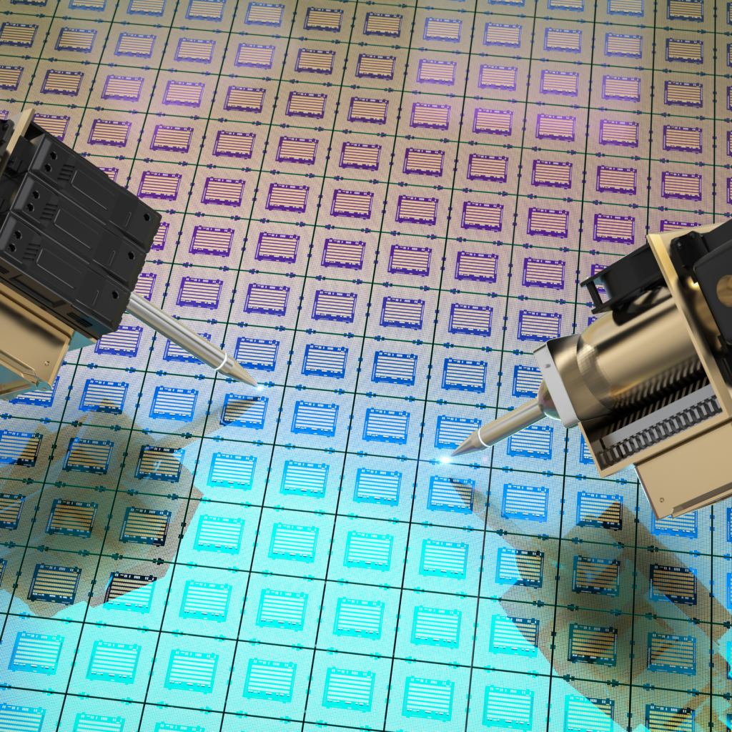
3 Fabrication and Manufacturing: As mentioned before this is a highly capital-intensive industry dependent on high production volumes from Semiconductor companies and with technological changes prone to obsolescence. A new Fab facility for 3 nanometer Semiconductor manufacture can easily cost over US$ 10 billion, would need 2-3 years from design to production, and become obsolete in 10 years. With its present budget, the GOI could invest in a maximum of two world-class fabs, without creating substantial employment or getting any IPR. In any case, due to the conflict between the USA, Taiwan, and Japan with China, several new fabs are coming up in the USA, Europe, and South East Asia. Intel just delayed the construction of its new Fab in Arizona as they foresee a glut in the market in 2-3 years. India and Indian companies should not be worried about having a Fab in India, there are enough companies who would be happy to manufacturefor us.
4 Packaging and Assembly: Once the die/IC is cut out from the wafer in the Fab, it is sent to a Packaging and Assembly facility. Here it is packed and assembled in plastic or ceramic, some components may be added and then soldered onto a substrate. This facility is also used for testing. Micron Technology Inc. of the USA has started construction of such a facility in Gujarat in two phases. As per press reports, Micron will Assemble and Test, DRAM, NAND, NOR memory, and storage chips. There is no IPR transfer. The total project cost is a whooping US$ 2.75 Billion with a 70% Subsidy from GOI and Govt. of Gujarat amounting to US$ 2 Billion, creating just 5000 direct jobs (approximately Rs 3 crores to create one technical job).
The Design Linked Incentive scheme of GOI, has a very small budget and shall be under the CDAC Umbrella. Startup promoters are independent thinkers, need least interference and management control and are passionate about their dreams. In the new schee of things, Startups shall be fettered and spend time navigating a bureaucratic quagmire. The GOI has no experience in evaluation, conception and incubating of startups. They do not have global industry perspective and connections as well as linkages for taking start-ups public internationally. The Govt. in all humility has no business to be in this business!
Here is what we can do.
Initially, China, had no VC, Startup Culture. They actively wooed Silicon Valley investors such as Sequoia, IDG, GGV, and Tiger Global to come to China and set up funds technology companies in China. Having learnt from Today China is an emerging super power in Semiconductors with an indigenous VC ecosystem and the Chinese Govt participates in Semiconductor investments alongwith.
US Silicon Valley, VCs have experience in seeding the Semiconductor industry right since Fairchild Semiconductor got US$1.4 million in 1957 and Intel got invested by angels in 1968 and went public in two years raising US $ 6.8 Million. They have over sixty years of experience in this sector. Let us use it.
The GOI, could act like a Limited Partner and provide say US$ 2 – 5 Billion to one to three such VCs. VC funds work on a 2-20 model. This means they charge the initial investor (known as the Limited Partner; in our hypothetical case, the Govt of India) 2% of the fund value charged yearly to fund the costs of running the fund and up to 20% of the profits if the invested company merges, gets acquired or goes public. VC Investors like these have decades of experience, deep-dive market connections, global networking, risk-taking abilities, and a multidisciplinary team of experts. They can look at ideas, evaluate the probability of success, do due diligence on promoters, and create definitive investment agreements. After which they can mentor founders, participate in the management, tweak business models, go to market, get companies merged, acquired, or go public.
Many invested companies will go bust while a few become unicorns or super unicorns. Start-ups who have technical skills and skin in the technology game should get the first option to get funds for setting up Chip Design and Marketing companies instead of large conglomerates whose promoters have no personal passion or technical ability in Semiconductors. Since the founders would not be able to bring in substantial capital initially, the ” GOI” could give them Sweat Equity from the Subsidy pool. The founders could also get money from the VCs if their business models are robust. The balance amount of Subsidy money would become Equity for the GOI (without shackling the day-to-day operations of the promoters and VC’). With US$ 2-5 Billion in the pot, one could fund about 20-30 companies to become Semiconductor Design and IPR owners.
An example. Nvidia is today a US$ 1 Trillion market capital company. It was formed in 1993. It does not own any Fab or Assembly plant. The founders realized that there was a market for Graphic Processing Chips for PCs and Workstations for Gaming and Computer Aided Design. They put in US$ 40,000 and later Sequoia put in US$ 20 million. By 1999-2000 Nvidia got a US$ 200 million advance for their Graphic chips for the X Box gaming console from Microsoft. By 2011, their chips were incorporated into mobile phones. In 2017, Nvidia realized that their GPU Chips could be used in AI processing for the emerging Large Learning Models such as ChatGPT. Microsoft, Amazon, Meta, Google, and nearly all AI companies invested heavily in their A100 and H100 Chipsets. Today more than 70% of AI processing is done by Nvidia chipsets. Not everyone shall become a Nvidia, but this should be an inspiration for Indian Semiconductor design companies.
Another example, Apple has a market cap of US $ 2.9 Trillion. TSMC which makes chips for them and others has a market cap of US$ 620 Million and Foxconn which assembles products for Apple has a market cap of just US$ 70 Billion. Apple conceives, designs, and sells products. They do not invest in fixed assets.
In conclusion, India has trained manpower working in Semiconductor design and money should be spent on creating IPR.
The investment in Micron Technologies goes against the concept of how wealth is created in the Knowledge Economy. However, it is not too late. Young Indian startups have the ability and passion to become world leaders in the Semiconductor industry.
Carpe Diem!
Leave a Reply